(Hong Kong)

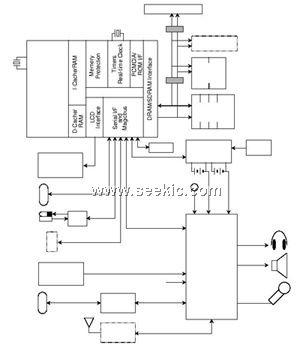
Product Summary
Plastic LQFP208-pin package (TMPR3912AU-92)
FBGA 217-pin package (TMPR3912XB-92)
Plastic LQFP176-pin package (TMPR3911BU)
FBGA177-pin package (TMPR3911BXB)
32-bit TX39/H Processor core, cache memory, multiply-accumulate module, multi-channel DMA
controller, bus interface unit and memory controller, power management, and other peripheral
subsystems all on a single integrated chip
minimal number of inter-chip connections
Maximum operation frequency: 58 MHz (TMPR3911BU and TMPR3911BXB)
92 MHz (TMPR3912AU-92 and XB-92)
low power consumption
entire TMPR3911/12 operation is 3.3 V (in case of TMPR3911BU/BXB, I/O: 3.3 V,
internal: 2.6 V)
real-time clock based on 32.768 kHz reference
Processor core clock stop state for low standby current
power-down modes for individual internal peripheral modules
Features
Processor core Module
TX39/H Processor core
full 32-bit operation (registers, instructions, addresses, etc.)
32 general purpose 32-bit registers; 32-bit program counter
MIPS RISC Instruction Set Architecture (ISA) supported
Translation Look-aside Buffer (TLB) (4K Page size, 32 entries)
on-chip cache
4 Kbyte instruction cache (I-cache)
physical address tag and valid bit per cache line
programmable burst size
instruction streaming mode supported
direct-mapped
1 Kbyte data cache (D-cache)
physical address tag and valid bit per cache line
programmable burst size
write-through
two-way set associative
cache address snoop mode supported for DMA
4-level deep write buffer
high-speed multiplier/accumulator
on-chip hardware multiplier
supports 32× 32 multiplier operations, with 64-bit accumulator
existing multiply instructions are enhanced and new multiply and add instructions are added to the
R3000A instruction set to improve the performance of DSP applications
Processor core interface
handles data bus, address bus, and control interface between Processor core and rest of the
TMPR3911/12
Diagrams